During the past few years a number of excellent designs have been published for domestic audio amplifiers. However, some of these designs are now rendered obsolescent by changes in the availability of components, and others intended to provide levels of power output which are in excess of the requirements of a normal living room. Also, most designs have tended to be rather complex.
In the circumstances it seemed worth while to consider just how simple a design could be made which would give adequate output power together with a standard of performance which was beyond reproach, and this study has resulted in the present design.
Output power and distortion
In view of the enormous popularity of the Mullard "5-10" valve amplifier, it appeared that a 10-watt output would be adequate for normal use; indeed when two such amplifiers are used as a stereo pair, the total sound output at full power can be quite astonishing using reasonably sensitive speakers.
* For today's speakers and expectations, this is clearly not the case. 10 Watts is likely to be sufficient for tweeters in a tri-amped system however, and this is the reason for publication of this circuit.
The original harmonic distortion standards for audio were laid down by D. T. Williamson in a series of articles published in Wireless World in 1947 and 1949; and the standard, proposed by him, for less than 0.1% total harmonic distortion at full rated power output, has been generally accepted as the target figure for high-quality audio power amplifiers. Since the main problem in the design of valve audio amplifiers lies in the difficulty in obtaining adequate performance from the output transformer, and since modern transistor circuit techniques allow the design of power amplifiers without output transformers, it seemed feasible to aim at a somewhat higher standard, 0.05% total harmonic distortion at full output power over the range 30Hz-20kHz. This also implies that the output power will be constant over this frequency range.
Circuit design
The first amplifier circuit of which the author is aware in which a transformerless transistor design was used to give a standard of performance approaching that of the "Williamson" amplifier, was that published in Wireless World in 1961 by Tobey and Dinsdale. This employed a class B output stage, with a series connected transistors in quasi-complementary symmetry. Subsequent high-quality transistor power amplifiers have largely tended to follow the design principles outlined in this article.
The major advantage of amplifiers of this type is that the normal static power dissipation is very low, and the overall power-conversion efficiency is high. Unfortunately there are also some inherent disadvantages due to the intrinsic dissimilarity in the response of the two halves of the push pull pair (if complementary transistors are used in asymmetrical circuit arrangement) together with some cross-over distortion due to the I c /V b characteristics. Much has been done, particularly by Bailey, to minimise the latter.
An additional characteristic of the class B output stage is that the current demand of the output transistors increases with the output signal, and this may reduce the output voltage and worsen the smoothing of the power supply, unless this is well designed. Also, because of the increase in current drive with output power, it is possible for a transient overload to drive the output transistors into a condition of thermal runaway, particularly with reactive loads, unless suitable protective circuitry is employed. These requirements have combined to increase the complexity of the circuit arrangement, and a well designed low- distortion class B power amplifier is no longer a simple or inexpensive thing to construct.
* The thermal runaway referred to is now known to be secondary breakdown, where the transistor suffers from a localised heating on the silicon die. This effect is very rapid, and can lead to almost instantaneous destruction of a transistor. This is one reason that MOSFETs are preferred by many amplifiers designers (the editor is not one of these!).
An alternative approach to the design of a transistor power amplifier combining good performance with simple construction is to use the output transistors in a class A configuration. This avoids the problems of asymmetry in quasi- complementary circuitry, thermal runaway on transient overload, crossover distortion and signal-dependent variations in power supply current demand. It is, however less efficient than a class B circuit, and the output transistors must be mounted on large heat sinks.

A 10-W Design giving subjectively better results than class B transistor amplifiers
The basic class A construction consists of a single transistor with a suitable collector load. the use of a resistor, as in Fig 1(a), would be a practical solution, but the best power-conversion efficiency would be about 12%. An l.F. choke, as shown in Fig1(b), would give much better efficiency, but a properly designed component would be bulky and expensive, and remove many of the advantages of a transformerless design. The use of a second, similar, transistor as a collector load, as shown in Fig 1(c), would be more convenient in terms of size and cost, and would allow the load to be driven effectively in push-pull if the inputs of the two transistors were of suitable magnitude and opposite in phase. This requirement can be achieved if the driver transistor is connected as shown in Fig. 2.

This method of connection also meets one of the most important requirements of a low distortion amplifier :- that the basic linearity of the amplifier should be good, even in the absence of feedback. Several factors contribute to this. There is the tendency of the Ic / Vb non-linearity of the characteristics of the output transistors to cancel, because during the part of the cycle in which one transistor is approaching cut-off the other is turned full on. There is a measure of internal feedback around the loop Tr1 Tr2 Tr3 because of the effect which the base impedance characteristics of Tr1 have on the output current of Tr3. Also, the driver transistor Tr3, which has to deliver a large voltage swing, is operated under conditions which favour low harmonic distortion :- low output load impedance, high input impedance.
* A potentially worthwhile improvement to this circuit is the addition of a 0.1 ohm resistor in the emitter circuit of Tr1. This applies local feedback to the entire gain stage, providing a significant reduction in distortion. If used, this should be a 5 Watt wirewound type to handle the current.

A practical power amplifier circuit using this type of output stage is shown in Fig. 3.
* The upper transistor (Tr2) is operating as a current source, whose output current is modulated. This allows the circuit to operate at about half the quiescent current that would be required if no modulation were applied. The values for R1 and R2 must be selected, based on the gain of Tr3. For a 40 Volt supply, if Tr3 were to have a gain of 50 at 1A, then ...
(R1 + R2) = 20V / 20mA (base current) = 1000 ohms. One problem with this approach is that the current provided by Tr2 will vary with temperature. Readers wishing to experiment with this circuit should ensure that the current is checked at normal operating temperature (i.e. HOT). There is no mechanism in the circuit to prevent thermal runaway, other than the use of a suitably large heatsink. At some point, the circuit should stabilise the quiescent current. If it does not (and the current continues to increase), then the heatsink is too small. To ensure a useful life for the transistors, they should not operate at greater than 50o C, which in normal conditions should be quite achievable. Since each transistor operates at (or near) 25 Watts, the heatsink for each transistor should have a thermal capacity of about 1o C / Watt. A better (i.e. larger) heatsink will do absolutely no harm, and will ensure freedom from thermal runaway.
There is also a newer version of this amp, but I have no plans to re-publish at any time.
The open loop gain of the circuit is approximately 600 with typical transistors. The closed loop gain is determined, at frequencies high enough for the impedance of C3 to be small in comparison to R4, by the ratio (R3 +R4)/R4. With the values indicated in Fig. 3, this is 13. This gives a feedback factor of about 160 milliohms.
Since the circuit has unity gain at D.C., because of the inclusion of C3 in the feedback loop, the output voltage Ve, is held at the same potential as the base of Tr4 plus the base emitter potential of Tr4 and the potential drop along R3 due to the emitter current of this transistor. Since the output transistor Tr1 will turn on as much current as is necessary to pull Ve down to this value, The resistor R2, which together with R1 controls the collector current of Tr2, can be used to set the static current of the amplifier output stages. It will also be apparent that Ve can be set to any desired value by small adjustments to R5 and R6. The optimum performance will be obtained when this is equal to half the supply voltage. (half a volt or so either way will make only a small difference to the maximum output power obtainable, and to the other characteristics of this amplifier, so there is no need for great precision in setting this.)
* Not mentioned is the purpose of C1 (in conjunction with R1 and R2). This capacitor provides "bootstrapping", which attempts to maintain a constant voltage across R2. If the voltage remains constant across a resistor, it follows that the current through the resistor must also remain constant. The performance of this circuit will be severely impaired if the value of C1 is too small - based upon the lowest frequency of operation, and the parallel value of R1 and R2. For operation down to 20Hz (assuming R1 + R2 = 1000 ohms), the capacitor should be at least 220uF.
Likewise, the reactance of C1 must be low with respect to the speaker impedance (preferably less than 1/2 of the speaker impedance at the lowest frequency of interest - 20Hz is assumed). This works out to be about 2,000uF. A working voltage of not less than 50V is suggested for all electrolytic capacitors, and for optimum h.f. performance, a 1uF polyester may be paralleled with each electro. In my experience this is not needed, but many will disagree, so if you want it, add it.
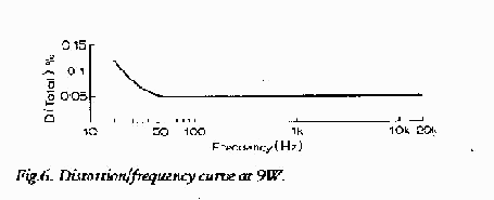
Silicon planar transistors are used throughout, and this gives good thermal stability and a low noise level. Also, since there is no requirement for complementary symmetry, all the power stages can use n-p-n transistors which offer, in silicon, the best performance and lowest cost. The overall performance at an output level of 10 watts, or at any lower level, more than meets the standards laid down by Williamson. The power output and gain/frequency graphs are shown in Figs. 4 and 5, and the relationship between output power and total harmonic distortion is shown in Fig. 6. Since the amplifier is a straight-forward class A circuit, the distortion decreases linearly with output voltage. (This would not necessarily be the case in a class B system if any significant amount of cross- over distortion was present.) The analysis of distortion components at levels of order of 0.05% is difficult, but it appears that the residual distortion below the level at which clipping begins is predominantly second harmonic.
Stability, power output and load impedance
Silicon planar NPN transistors have in general, excellent high frequency characteristics, and these contribute to the very good stability of the amplifier with reactive loads. The author has not yet found a combination of L and C which makes the system unstable, although the system will readily become oscillatory with an inductive load if R3 is shunted by a small capacitor to cause roll-off at high frequencies.
The circuit shown in Fig. 3 may be used, with very little modification to the component values, to drive load impedances in the range 3-15 ohms. However, the chosen output power is represented by a different current/voltage relationship in each case, and the current through the output transistors and the output voltage swing will therefore be different. The peak-voltage swing and mean output current can be calculated quite simply from the well-known relationship W=I2R and V=IR, where the symbols have their customary significance. (it should be remembered, however, that the calculation of output power is based on RMS values of current and voltage, that these must be multiplied by 1.41 to obtain peak values, and that the voltage swing measured is the peak to peak voltage, which is twice the peak value.)
When these calculations have been made, the peak-to-peak voltage swing for 10 watts power into a 15-Ohm load is found to be 34.8 volts. Since the two output transistors bottom at about 0.6 volts each, the power supply must provide a minimum of 36 volts in order to supply this output. For loads of 8 and 3 ohms, the minimum h.t. line voltage must be 27V and 17V respectively. The necessary minimum currents are 0.9, 1.2 and 2.0 amps. Suggested component values for operation with these load impedances are shown in table 1. C3 and C1 together influence the voltage and power roll-off at low audio frequency performance is desired than that shown in figs. 4 and 5.
* I suggest a power supply voltage of 40 Volts, which will actually allow close to 20 Watts into an 8 ohm load. Make sure that the heatsinks are sufficient to handle the additional power dissipation caused by the higher supply voltage. Those suggested in the construction notes are probably too small for operation at this supply voltage.


Since the supply voltages and output currents involved lead to dissipation in the order of 17 watts in each output transistor, and since it is undesirable (for component longevity) to permit high operating temperatures, adequate heat sink area must be provided for each transistor. A pair of separately mounted 125mm by 100mm (5" by 4") finned heatsinks is suggested. This is, unfortunately, the penalty which must be paid for class A operation. For supplies above 30V Tr1 and Tr2 should be Mj481s and Tr3 a 2n1613.
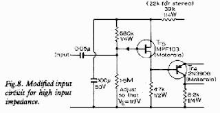
If the output impedance of the preamplifier is more than a few thousand ohms, the input stage of the amplifier modified to include a simple f.e.t. source follower circuit shown in fig 8. This increases the harmonic distortion to about 0.12%, and is therefore (theoretically) a less attractive solution than a better pre- amplifier.
A high frequency roll-off can be obtained, if necessary by connecting a small capacitor between the gate of the f.e.t and the negative (earthy) line.
Suitable transistors
Some experiments were made to determine the extent to which the circuit performance was influenced by the type and current gain of the transistors used. As expected the best performance was obtained when high-gain transistors were used, and when the output stage used a matched pair. No adequate substitution is known for the 2N697 / 2N1613 type used in the driver stage, but examples of this transistor type from three different manufacturers where used with apparently identical results. Similarly, the use of alternative types of input transistor produced no apparent performance change, and the Texas Instuments 2N4058 is fully interchangeable with the Motorola 2N3906 used in the prototype.
The most noteworthy performance changes were found in the current gain characteristics of the output transistor pair, and for the lowest possible distortion with any pair, the voltage at the point from the loudspeaker is fed should be adjusted so that it is within 0.25 volt of half the supply line potential.
The transistors used in these experiments were Motorola MJ480/481, with one exception, in which Texas 2S034 devices were tried. The main conclusion which can be drawn from this is that the type of transistor used may not be very important, but that if there are differences in the current gains of the output transistors, it is necessary that the device with the higher gain shall be used in the position Tr1.
When the distortion components were found prior to the onset of waveform clipping, these were almost wholly due to the presence of second harmonics.
Constructional notes
Amplifier
The components necessary for a 10 + 10 watt stereo amplifier pair can be conveniently be assembled on a standard 'Lektrokit' 4" X 4.75" s.r.b.p. pin board, with the four power transistors mounted on external heat sinks. Except where noted the values of components do not appear to be particularly critical, and 10% tolerance resistors can certainly be used without ill effect. The lowest noise levels will however be obtained with good quality components, and with carbon-film or metal-oxide resistors.
* Metal film resistors should be used throughout, as these are superior to carbon film types in all respects. These are generally only available as 1% or better tolerance, which will not pose any problems.
Power supply
A suggested form of power supply unit is shown in Fig. 9(a). Since the current demand of the amplifier is substantially constant, a series transistor smoothing circuit can be used in which the power supply output voltage may be adjusted by choice of the base current input provided by the emitter follower Tr2 and the potentiometer VR1. With the values of the reservoir capacitor shown in table 3, the ripple level will be less than 10mV at the rated output current, provided that the current gain of the series transistor is greater than 40. For output currents up to 2.5 amps, the series transistors indicated will be adequate, provided that they are mounted on heat sinks appropriate to their loading.

However, at the current levels necessary for operation of the 3-ohm version of the amplifier as a stereo pair, a single MJ480 will no longer be adequate, and either a more suitable series transistor must be used, such as the Mullard BDY20, with for example a 2N1711 as Tr2, or with a parallel connected arrangement as shown in Fig. 9(b).
The total resistance in the rectifier "primary" circuit, including the transformer secondary winding, must not be less than 0.25 Ohms. When the power supply, with or without an amplifier, is to be used with an r.f. amplifier-tuner unit, it may be necessary to add a 0.25uF (160V) capacitor across the secondary windings of T1 to prevent transient radiation. The rectifier diodes specified are International Rectifier potted bridge types.
* This supply is not a regulated supply, but is a simple capacitance multiplier. For a more complete description of a better circuit, see Capacitance Multiplier Power Supply Filter in these pages.
Current Limiting
* Although there was no mention of this in the original article (and I managed to "lose" the schematic file for a time), a current limiter was included. This will ensure that the current through the output devices does not exceed a preset value, although I believe that the concept is flawed, and is of limited value in this overall design.

The circuit above shows the way the current limiter is connected. It will not stabilise the quiescent (no signal) current, but is only capable of ensuring that the absolute maximum current does not exceed the value determined by the 100 Ohm pot. To be useful, a current stabiliser is needed, which will ensure that the no-signal operating current remains constant regardless of temperature or supply voltage variations. No information is provided to achieve this goal.
Additional Notes
This article (with editorial notes) is reprinted as a service to readers, who are reminded of copyright laws, which may restrict the rights of readers for reproduction, commercial production (etc). The information presented is not intended as a guide for construction, but is primarily for its interest value, and to serve as a starting point for other designers.
The original article is now many years old, and some of the transistor types referred to are now superceded by vastly better designs. I will leave it to readers to experiment with device types. While much of the design is still quite relevant to a new design, I think that this amplifier may be found lacking compared to more recent design trends. In particular, the biasing system is not stable with temperature, and DC drift will be evident. In addition, the open-loop gain is very low, so feedback is far less than might be desirable (although many will feel that this is a good thing!). As mentioned above, additional local feedback (0.1 ohm resistor in the emitter of Tr1) may reduce open-loop distortion, but further reduces the gain. I suggest experimentation (I have only done some computer simulations so far) and would appreciate feedback from anyone who tries out this circuit.
I would also suggest that a single supply power amplifier is not really a proposition for new designs (although the DoZ uses the same principle), and a bi-polar (+/-) power supply may be preferable. DC stabilisation then becomes a major issue, since small DC offset voltages can prove a disaster to tweeters in particular.
The diagrams are not of high quality, but are the originals from the source WWW page. I do not propose to redraw these, as this design is provided as information only.
The Author
John L Linsley-Hood is a prolific author of amplifier designs, and still presents new ideas and circuits in the UK magazine Electronics World (formerly Wireless World). His influence on the design of quality audio amplifers has been considerable, and continues to this day. This is not to say that I agree with or endorse all his ideas or theories, but at least he has the guts to say what he thinks, and the magazine has the guts to print it, too.